Absorption microscopes
We offer a novel, ultra-sensitive raster-scanning absorption microscope for the detection and quantitative characterization of nanoscale particles, low-dimensional materials, thin films, and defects in vacuum, air, and liquid environments.
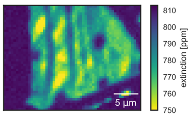
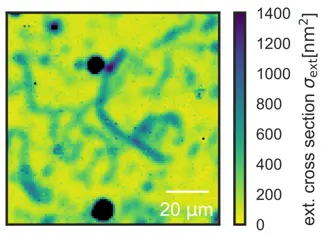
In this system, conventional lenses and objectives are replaced by a pair of high-reflectivity mirrors, significantly enhancing light–matter interaction. One mirror is macroscopic and serves as the sample substrate, while the second is microscopically small. By raster-scanning the sample with high speed and precision, the system generates absorption images with unprecedented sensitivity—down to 0.1 parts per million—exceeding the performance of conventional techniques by a factor of 1,000. This capability reveals optically "invisible" samples, such as individual nanoparticles, single defects, and even single molecules.
The microscope is capable of imaging areas up to 300 × 300 µm² within a few seconds, achieving diffraction-limited spatial resolution. At a fixed point, time-resolved measurements can be performed with a temporal resolution on the order of a few microseconds.
Each mirror set provides a spectral bandwidth of 100–150 nm. A wide selection of stock and custom mirrors is available, all of which can be exchanged in under 30 minutes, allowing full coverage of the visible to near-infrared (VIS/NIR) spectral range.
Control is managed through a Python-based software suite that includes standard measurement and analysis routines. The software also supports integration with additional laboratory instrumentation.
The microscope is also highly sensitive to scattering and also support fluorescent imaging, dielectric index and phase measurements as well as polarization control.
For advanced spectroscopic applications, an optional module enables high-resolution spectroscopy with spectral resolution down to 0.02 nm in under one second, as well as the acquisition of hyperspectral maps.
Performance specs
ΔA<0.0001%
Ultra sensitive
Δt<1ms
Time resolution
0.1mm²
Image size
1 FPS
Fast imaging
Δλ 150nm
Hyperspectral maps
350-2000nm
Broad spectral range
Features

FULL INSIGHT
Characterize individual nanoparticles, single defects and thin films on an unprecedented level with ultra-sensitive microscopy and hyperspectral imaging.

FULL CONTROL
Measurement and analysis modules in Python for easy and fast data acquisition and integration with your lab routines.

FULL SUPPORT
Close support by experts from the design of the experiment till the publication.
Applications
Our microscope can image and measure a wide range of materials, prepared using techniques such as spin-coating, drop-casting, stamping, and more.
2D materials
See variations of absorption, scattering and polarization on 0.0001% levels in atomically thin materials
Carbon nanotubes
Visualize and perform absorption spectroscopy on single carbon nanotubes
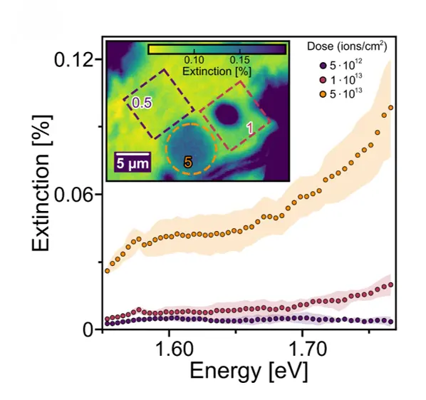
Defects
Absolute absorption cross sections of atomistic defects can be measured
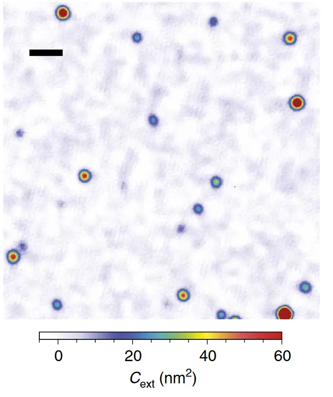
Nano-particles
Measure presence, spectra, distribution and location of nanoparticles, e.g. nm-sized gold or Perovskites.
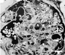
Tissue & Sections
Image few nm-thick sections of tissue or ultra-thin sections of cells.

Your material
Microscope comparison
Image of an unstained ultra-thin (~ 80 nm) section of a human kidney biopsy in:
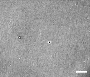
a brightfield
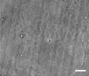
a phase contrast light microscope

a resonator microscope
Use our technology as a Pilot User
Be the first to try our new technology by becoming a pilot user. We will work together with you to make visible what has been hidden so far. Just contact us!
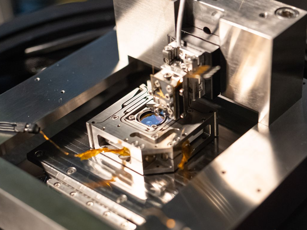
Scanning cavity technology
How our scanning cavity microscope works:
Funded by the European Union
We are proud that this Project is funded by the competitive European Innovation Council under a EIC Transition Project (Grant agreement number 101146834). This is a program to fund highly innovative Ideas of SMEs to Validate technologies and develop business plans. It supports the maturation and validation of novel technologies from the lab to the relevant application environments.